
Where to start
- New to RTL entirely? Start with System Verilog for Design - combinational/sequential logic, D flip-flops, counters, shift registers - before anything else on this page will make sense.
- Comfortable with syntax, want structured daily practice? 21 Days of RTL (free) runs from a 2:1 mux up to round-robin arbiters over 21 days.
- Ready for interview-level design problems? Hands-on RTL Design is the flagship course this page draws from most - 26 modules, most of the patterns below map directly onto one of them.
Core topics checklist
Run through these before any interview - they cover the bulk of what gets asked.
- Basic mux-based converters - practice: Data Muxing
- Timing equations (setup/hold, Tclk-to-q, combinational delay budget)
- Out-of-order (OoO) execution concepts - see RISC-V Processor Design for the architecture context
- LRU cache replacement - practice: Least Recently Used (RTL Design), or in a real cache pipeline: VIPT Cache - Replacement Policy
- FIFO depth/size calculation
- Async FIFO design - related building blocks: Fast Fifo, Fifo Flush
- Converters: gray ↔ one-hot ↔ binary - closest hands-on practice: Big Endian Converter (same bit-remapping skill, different mapping)
- Counters (standard, Gray-code, modulo-N) - practice: Atomic Counters, Counter, Up-down Counter, Self Reloading Counter
Company-specific questions
Google - RTL Design Integration Engineer
- Fibonacci series in RTL
- Divide-by-5 RTL design (bonus: generalize to divide-by-N) - practice the same technique on Divide by 3, then generalize what you learn
- Low power design techniques - practice: Low Power Channel
- Sync a single pulse signal between two clock domains - practice: Two Pulses, Edge Capture, One Shot
- Sync multiple pulse signals between two clock domains - write the RTL. Two Pulses is built around exactly this problem.
- Design problem - in-order response reordering:
A block receives requests from unit A, buffers them, does some processing, dispatches to memory, waits for responses, and sends them back to A. Constraint: request order = response order.
Given 4 requests (r1, r2, r3, r4) arriving and dispatched in that order, memory responds out of order - r3, r2, r1, r4. Design the block so responses are still returned to A in the original order: r1, r2, r3, r4.
This is almost exactly Ordering - Credits & Deadlock covers the buffering/backpressure half of the same problem.
Microsoft - Packet RX/TX buffer design
Design a block that receives streamed packet data, buffers it, and retransmits it - with the constraint that if the internal buffer fills, all previously-accumulated blocks of the current packet must be dropped, and the block waits for a new SOP.
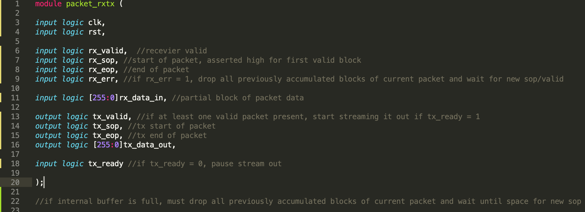
module packet_rxtx (

  input logic clk,
  input logic rst,

  input logic rx_valid,        // receiver valid
  input logic rx_sop,          // start of packet, asserted high for first valid block
  input logic rx_eop,          // end of packet
  input logic rx_err,          // if rx_err = 1, drop all previously accumulated blocks
                                // of current packet and wait for new sop/valid

  input logic [255:0] rx_data_in,   // partial block of packet data

  output logic tx_valid,       // if at least one valid packet present, start streaming
                                // it out if tx_ready = 1
  output logic tx_sop,         // tx start of packet
  output logic tx_eop,         // tx end of packet
  output logic [255:0] tx_data_out,

  input logic tx_ready         // if tx_ready = 0, pause stream out
);

// if internal buffer is full, must drop all previously accumulated blocks
// of current packet and wait until space for new sop
(Port list transcribed from the screenshot, which cuts off after the buffer-full comment - reconstruct the FSM and buffer management from the spec.)
This exact problem shape - drop-on-full packet buffering - is the spine of Hands-On RTL design for Networking Systems. Closest modules: Drop the Garbage (the buffer-full-drop behavior, directly), Handling Traffic and Handling Traffic 2, Scatter and Gather. In the RTL Design course: Buffering, Packet Decoder, Complex Packet Decoder.
Clock domain crossing (CDC)
2-stage synchronizer - how it actually resolves metastability
Assumptions: input is asynchronous, starts at 0 (so Q1 = Q2 = 0), then transitions to 1.
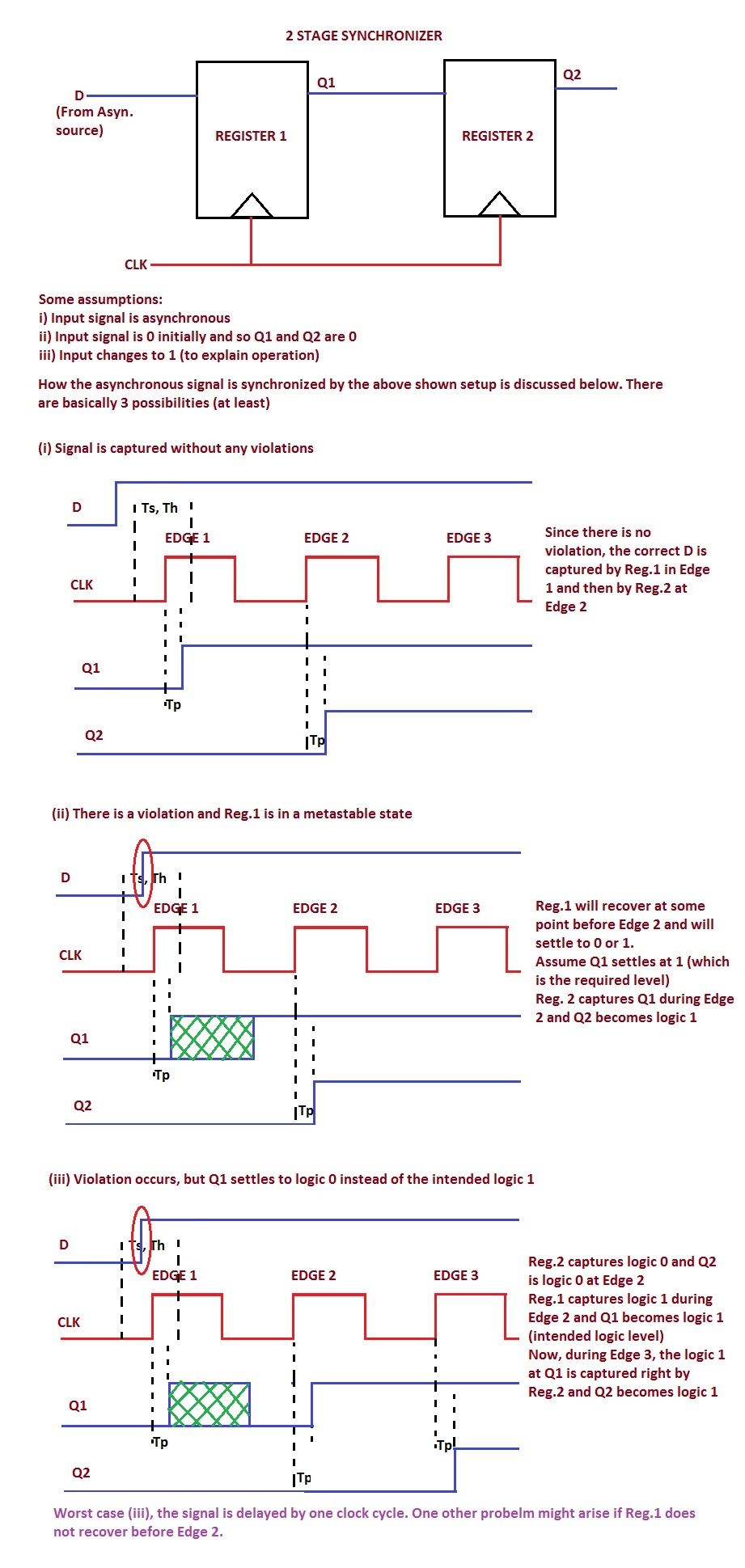
Three outcomes when D changes near a clock edge:
- No violation - D is captured cleanly by Reg1 on Edge 1, then by Reg2 on Edge 2. No metastability.
- Violation, Reg1 goes metastable, but resolves before Edge 2 - Reg1 settles to 1 (the correct value) before the next edge, so Reg2 captures it cleanly on Edge 2. Correct result, no extra latency.
- Violation, Reg1 resolves to the wrong value first - Reg1 settles to 0 instead of 1, so Q2 is wrong at Edge 2. Reg1 then captures the still-present 1 on Edge 2, and Q2 finally becomes correct at Edge 3 - a one clock-cycle delay in the worst case.
The unhandled failure mode: if Reg1 does not resolve before Edge 2 at all, the metastability propagates further downstream - this is why synchronizer timing margin (MTBF) matters, not just adding two flops and calling it done.
Practice on QuickSilicon: Two Pulses, Edge Capture, One Shot, Clock Generator, Asynchronous Resets
CDC background reading: Cummings, SNUG 2008 - Clock Domain Crossing (CDC) Design & Verification Techniques
AXI interview questions
- How would you do an async clock-domain crossing for AXI?
- How would you merge 2 AXI interfaces (2 masters talking to the same slave)? - the underlying skill is arbitration: practice Single Cycle Arbiters
- How would you split an AXI interface (1 master talking to 2 slaves)?
- Combine the above: 2 masters, each independently able to reach 2 slaves
- How would you add a register slice between a master and a slave? - a register slice is a skid buffer: practice Skid Buffer
- A master issues multiple outstanding transactions - pros/cons of using the same ID for all vs. a different ID for each?
- Where is AXI actually used, and how does it differ from APB? - build APB end-to-end to ground the comparison: Events to APB (design side), or the full verification-side APB stack in Hands-on Testbench Design (APB Interface → APB Driver → APB Monitor → APB Scoreboard)
- What is register slicing? - see Skid Buffer above
- What is a split transaction?
- Valid/ready sequencing on read and write channels - the same handshake trained in Skid Buffer
- TrustZone protection bits - what are they for?
Low power design
Static power
- Multi-Vt design - don't use faster (leakier) cells where timing slack already exists
- Power gating
Dynamic power
- Multi-bit registers (bank multiple flops to share clock/logic overhead)
- Clock gating, applied at multiple levels of hierarchy, driven by RTL structure
- Reduce switching activity on high-activity signals by restructuring logic
- Capacitance reduction: lower drive-strength cells, lower metal layers where routing allows - reduces pin cap, at some leakage cost
- DVFS (dynamic voltage/frequency scaling)
Practice on QuickSilicon: Low Power Channel, Power Saving (networking-context low power)
Bug class → what actually catches it
A recurring interview question: "how would you have caught this bug?" Map the failure to the tool, not to "more testing." (Unfamiliar term? Check the QuickSilicon Glossary.)
| Bug class | Caught by |
|---|---|
| Setup/hold violation | STA |
| CDC errors | CDC tool |
| Clock skew | STA |
| X-propagation | Xprop simulation at RTL |
| Uninitialized signals | Formal reset checks |
| Latches (unintended) | Lint tool |
| Incorrect power-up / reset sequencing | UPF-aware simulation (e.g. VCLP-style) |
| Synthesis optimization / tool errors | LEC (logic equivalence checking) |
GLS is the catch-all for what falls through the above - but a GLS-only catch usually signals a process gap further upstream. Wrong timing constraints in particular have no dedicated check unless GLS is run.
SystemVerilog / verification notes
- Race-condition fix: unless a specific construct requires otherwise, use
#0to postpone a check into the Postponed region rather than checking in the current Active time step. This is the simplest fix - and also the weakest one; understand why the race exists before reaching for#0reflexively. - SystemVerilog.io - race condition challenge, worked responses
- SystemVerilog.io - full tag index
Constrained-random / SVA practice on QuickSilicon: Hands-on Testbench Design includes a set of DVCon '26 Hackathon constraint problems that are exactly this skill - Frequency Constraint, Five Consecutive Ones, Grouped Ones, Non Adjacent Ones, Weighted Popcount.
Curated resource library
QuickSilicon courses, by topic
| Topic | Course |
|---|---|
| RTL design patterns, arbiters, FIFOs, converters, low power | Hands-on RTL Design |
| SystemVerilog testbenches, APB, UVM-style verification, constrained-random | Hands-on Testbench Design |
| Computer architecture, RISC-V pipeline (fetch/decode/execute/branch) | RISC-V Processor Design |
| Caches, the 3 Cs model, replacement policy, SRAM macros | VIPT Cache Design |
| Packet processing, parsers, checksums, traffic shaping | Hands-On RTL design for Networking Systems |
| Absolute basics: combinational/sequential logic, flops, counters | System Verilog for Design |
| Free 21-day structured practice track | 21 Days of RTL |
Digital logic fundamentals
- Fundamentals of Digital Circuits - Anand Kumar
- Digital design practice set - MUX-based gate design, FSMs, clock/frequency dividers, sequence detectors/generators, edge detectors, encoders
Static timing analysis (STA)
- STA basics overview
- STA - basic timing checks
- What is meant by constraints
- Inputs/outputs of ASIC synthesis
- SDC - Synopsys Design Constraints
- Setup and hold checks, part II
Clock domain crossing / reset domain crossing
- CDC interview-focused primer
- Clock crossing (UC Berkeley CS150)
- CSU Ohio - RTL chapter 16 slides on CDC
- Cummings, SNUG 2003 - Resets
- 4-phase CDC pulse synchronizer
- No Man's Land - CDC edge cases
Async FIFO
- Cummings, SNUG 2002 - Async FIFO design, part 1
- FIFO depth calculation - asked very frequently
SystemVerilog Assertions (SVA)
UPF / low power implementation
Verification / UVM
- Verification Guide - UVM
- Verification methodology YouTube channel
- ASIC verification & testing - course chapter (UT Dallas)
Valid/ready handshake
Computer architecture
- General computer architecture
- General computer architecture (alt.)
- Quick overview series (YouTube, 4 parts) - good if short on time
- Virtual memory
- Parallel computer architecture - comprehensive reference
- Core topics to know cold: caches, the 3 Cs model, cache replacement schemes, pipeline hazards, reorder buffer, virtual memory, cache coherence protocols
Good-to-know / down-the-stack
- Resource 1 - some less-common concepts explained well
- Resource 2 - worth going down the stack on this too
- Master prep document (Google Doc, kept updated)
Semiconductor blogs worth following
Most semiconductor blogs that surface on Google are corporate content optimized for SEO. These actually add value:
- CPU/GPU deep-dive blog - authors go by "Nexus" and "Clamchowder"
- SemiAccurate - processor-focused, Charlie Demerjian
- SemiAnalysis - Dylan Patel, deep dives on semi business/operational strategy
- Fabricated Knowledge - Doug O'Laughlin, long-form investment-angle primers
- The Memory Guy - Jim Handy on memory and storage
Sourced from a personal interview-prep collection, reorganized and cross-linked to QuickSilicon course modules. Company question attributions reflect the original source's recollection, not a guarantee of current interview content.
Subscribe to the free QuickSilicon newsletter.
Subscribe to the newsletter